

STM32-ADS1256 ARM Development Board ADS1256+STM32F103C8T6 ADC power supply 24-bit .
Specifications:
1. Chip model: STM32F103C8T6 (microcontroller), ADS1256 (24 bit Precision AD conversion chip)
2. Power supply voltage: onboard 5V and 3.3V voltage regulator components, 9V external direct Current Power supply, the power supply has the function of preventing reverse connection.
3. Crystal frequency: 8MHZ, 9 times the frequency inside the chip, working frequency 72MHZ
4. Work Temperature: -25℃~85℃
5. Work Humidity: 5%~95%RH
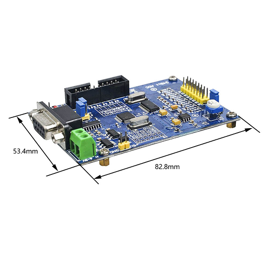
6. Dimensions 82.8*53.4*1.6mm
Features :
1. This board has designed all the lO ports ‘out’ on the STM32F103C8T6 microcontroller, Users can re-develop the functions they need;
2. You can download the program through the serial port, see the instruction file for the specific method.
Because it can Download the program through the serial port, so there is no JLINK download and debug interface on the board;
3. The reference voltage of the AD chip is 2.5V, which is generated by a precision voltage regulator device;
4. There is a potentiometer on the board to test the AD input. This potentiometer is divided by voltage. The generated voltage is connected to AN0 through the S3 jumper, which is suitable when there is no sensor Debug the board under the circumstances. If you don' t need this test, you can take the S3 jumper If the test voltage is turned off, input the test voltage directly from AN0--AN7. (Input to AD input voltage of the terminal cannot be higher than 5V).
The specific functions of the three modes are described below:
// Mode 1:
The single-channel AN0 analog voltage is continuously collected for ADC conversion, and the converted data is calculated as the voltage value, and the data is sent through the serial port in the form of ASCII code. In this mode, serial port assistant software can directly read the voltage, which is suitable for software development engineers, because there is no need to understand any principle of SCM hardware.
The collected data shows the following example. This time, the voltage is connected to Di0 channel (AN0), and the measurement accuracy is very stable within the range of 0.0001V(i.e. 0.1MV).The rest of the passageway is empty.
Because the transmission is ASCII code, so the host computer serial port software should choose "character (ASCII) display", do not choose hexadecimal display, otherwise display disorderly code.
// Mode 2:
The 8-channel analog voltage is continuously collected for 24-bit ADC conversion, and the converted data is calculated as the voltage value, and the data is sent through the serial port in the form of ASCII code. In this mode, serial port assistant software can also be used to directly read the voltage, suitable for software development engineers to use, because there is no need to understand any principle of SCM hardware.
The collected data are shown as follows:
// Mode 3:
Full differential input mode, voltage range measured is -5V~+5V. Total 4 sets of differential inputs. Sensors suitable for connecting electronic scales.
The corresponding input pin is:
AN0-- Channel 0(V0) + input
AN1-- Channel 0(V0) -- input
AN2---- Channel 1(V1) + input
AN3---- Channel 1(V1) -- input
AN4-- channel 2(V2) + input
AN5---- Channel 2(V2) -- input
AN6-- Channel 3(V3) + input
AN7-- channel 3(V3) -- input
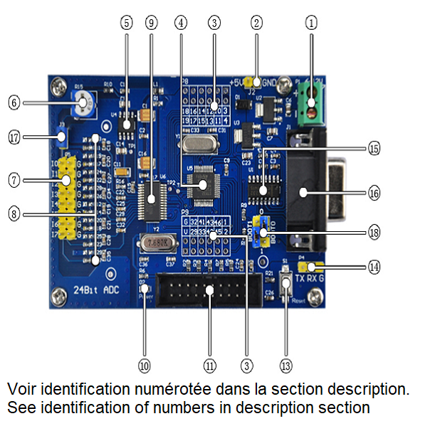
Numbered Identification
1. Power input terminal, input voltage range 5.5V-12V (5V power supply, please directly connect 2 can be);
2. 5V power supply input terminal (1.2 two power supplies, connect to either one only);
3. STM32F103C8T6 leads to GPIO, which is convenient for secondary development. Screen printing directly corresponds to the pin number of the chip;
4. New original master MCU: STM32F103C8T6;
5. 2.5V reference, ultra-high precision, low-temperature drift;
6. Adjustable potentiometer, output adjustable voltage link to AIN0/ I0;
7. 8 channels for acquisition input, I0-I7 is connected to the positive end of acquisition voltage, G is the analog ground, and is connected to the negative end of acquisition voltage;
8. Input filter and attenuation resistance, default no attenuation, leaving the position of welding attenuation resistance, 0603 package;
9. ADS1256IDB acquisition chip, brand new original import;
10. Power indicator LED;
11. JTAG interface, designed according to the definition of JLink-V8 or V9;
12. Not marked;
13. STM32F103C8T6 reset button;
14. USB to TTL wiring position, corresponding to TX, RX and GND of MCU, which can directly communicate with the computer;
15. Original imported 3232 serial port communication chip;
16. Serial head, female head;
17. On-off control of output voltage of adjustable potentiometer to I0 / AIN0: disconnect IO suspension and connect I0 to measure output voltage end of adjustable potentiometer;
18. STM32's BOOT0 and BOOT1 control jump cap.